INTRODUCTION TO CAPACITOR BANKS,
Table of Contents
- 1 DEFINITION OF AND CHARACTERISTICS OF CAPACITORS
- 2 USE OF CAPACITORS AND CAPACITOR BANKS
- 3 TRANSIENT DISTURBANCES AND HARMONICS
- 4 POWER FACTOR CORRECTION
DEFINITION OF AND CHARACTERISTICS OF CAPACITORS
A capacitor, also known as “condenser” is an electrical element with two electrical conductors separated by an insulator material (dielectric), as shown in Figure 1.
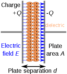
Figure 1 – Simplified scheme of a capacitor
The electric parameter that defines a capacitor is the “capacitance” (symbol: C) and the unit, according to International System of Units (SI), is “farad” (symbol: F).
The most common used dielectrics are:
- Ceramics
- Plastic films
- Oxide layer on metal (Aluminum; Tantalum; Niobium)
- Mica, glass, paper, air and other similar natural materials
- Vacuum
USE OF CAPACITORS AND CAPACITOR BANKS
In power electric systems capacitors and capacitors banks, which must be in accordance with IEC[1] Standards 60143 and 60871 or IEEE[2] Standard 824, are used to:
- Compensate reactive energy (power factor correction) due to consumers (MV and LV) and the inductive effect of long overhead lines and underground cables (MV and MV).
- Provide voltage regulation (HV[3]).
- Start of single phase squirrel cage motors (LV).
A shunt capacitor bank (or simply capacitor bank) is a set of capacitor units, arranged in parallel/series association within a steel enclosure.
Usually fuses are used to protect capacitor units and they may be located inside the capacitor unit, on each element, or outside the unit.
Capacitor banks may be star or delta connected. Delta-connected banks are generally used only in MV distribution networks and in LV installations.
Figure 2 shows what was explained above.

Figure 2 – Schematic diagram of a capacitor bank
Capacitors may retain a charge long after power is removed from a circuit; this charge can cause dangerous or even potentially fatal shocks or damage connected equipment.
Capacitors banks may have built-in discharge resistors to dissipate stored energyto a safe level within a few seconds after power is removed.
Capacitors banks shall be stored with the terminals shorted, as protection from potentially dangerous voltages due to dielectric absorption[4].
HV capacitor banks are installed outdoors, surrounded by a fence, and LV capacitor banks are installed indoors, in metallic enclosures (switchboards).
In MV installations capacitor banks may be installed either outdoors, surrounded by a fence or in the pole of a MV overhead line, or indoors, in metallic enclosures(switchgears).
The fence must have a lock with a delayed opening to assure the time requested for the complete discharge of the capacitors.
Examples of capacitor banks are shown in figures 3 and 4.
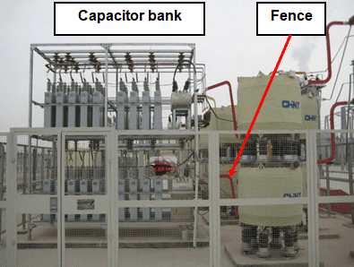
Figure 3 – HV Capacitor bank

Figure 4 – LV Capacitor bank
TRANSIENT DISTURBANCES AND HARMONICS
During electrical switching of capacitor banks, transient disturbances (during a short time) occur in power systems that may damage key equipment, potentially having a great impact on system reliability.
An oscillation of the power system and electromagnetic pulses (EMP) can be provoked by that sudden change of a circuit.
One of those transient disturbances is overvoltage (known as “switching overvoltages”) that influences the required insulation level of the network and of the equipments.
During the switching of capacitor banks, high magnitude and high frequency transients can occur.
The impedance of a circuit dictates the current flow in that circuit.
As the supply impedance is generally considered to be inductive, the network impedance increases with frequency while the impedance of a capacitor decreases. This encourages a greater proportion of the currents circulating at frequencies above the fundamental supply frequency (50Hz or 60 Hz) to be absorbed by the capacitor, and all equipment associated with the capacitor.
In certain circumstances such currents can exceed the value of the fundamental (50Hz or 60 Hz) capacitor current. These currents in turn cause increased voltage to be applied across the dielectric of the capacitor. The harmonic voltage due to each harmonic current added arithmetically to the fundamental voltage dictates the voltage stress to be sustained by the capacitor dielectric and for which the capacitor must be designed, to avoid additional heating and higher dielectric stress.
Capacitors may catastrophically fail when subjected to voltages or currents beyond their rating, or as they reach their normal end of life. Dielectric or metal interconnection failures may create arcing that vaporizes the dielectric fluid, resulting in that case bulging, rupture, or even an explosion.
Capacitors units are intended to be operated at or below their rated voltage and frequency.
IEEE Std. 18-1992 and Std 1036-1992 specifies the standard ratings of the capacitors designed for shunt connection to ac systems and also provide application guidelines. These standards stipulate that:
- Capacitor units should be capable of continuous operation up to 110% of rated terminal rms[5] voltage and a crest (peak) voltage not exceeding 2 x √2 of rated rms voltage, including harmonics but excluding transients. The capacitor should also be able to carry 135% of nominal current.
- Capacitors units should not give less than 100% and more than 115% of rated reactive power at rated sinusoidal voltage and frequency.
- Capacitor units should be suitable for continuous operation at up to 135% of rated reactive power caused by the combined effects of:
- Voltage in excess of the nameplate rating at fundamental frequency, but not over 110% of rated rms voltage.
- Harmonic voltages superimposed on the fundamental frequency: reactive powermanufacturing tolerance of up to 115% of rated reactive power.
If harmonic problems exist, they most often manifest themselves first at shunt capacitor banks in the form of audible noise, blown fuses or capacitor unit failures.
As frequency varies, so reactance varies and a point can be reached when the capacitor reactance and the supply reactance are equal. This point is known as the circuit resonant frequency.
Whenever power factor correction is applied to a distribution network, bringing together capacitance and inductance, there will always be a frequency at which the capacitors are in parallel resonance with the supply.
If this condition occurs at, or close to, one of the harmonics generated by any solid state control equipment, then large harmonic currents can circulate between the supply network and the capacitor equipment, limited only by the damping resistance in the circuit. Such currents will add to the harmonic voltage disturbance in the network causing an increased voltage distortion.
This result in an unacceptably high voltage across the capacitor dielectric coupled with an excessive current through all the capacitor ancillary components. The most common order of harmonics is 5th, 7th, 11th and 13th but resonance can occur at any frequency.
Capacitors can be effectively applied in these types of environments by selecting compensation levels that do not tune the circuit or by the use of a filter.
POWER FACTOR CORRECTION
In electrical installations, namely in industry, exists several consumers, such as motors, that have an important inductive load that provokes a phase shift between voltage and current, as show on the figure below.
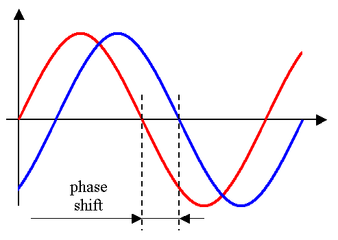
Figure 5 – Phase shift
Phase shift is represented as an angle (Ф) and current may be in advance or delayed of voltage.
If capacitance of the circuit prevails current is advanced; if inductance prevails current is delayed.
This phase shift provokes that “useful power” (active power – unit: W or kW) is lowerthan the power supplied (apparent power – unit: VA or kVA), the difference being the reactive power – unit: VAr or kVAr.
Representing those powers by vectors, the “power triangle” may be as shown on the figure below.
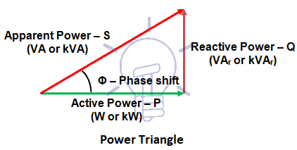
Figure 6 – Power triangle
P = S x cos Φ
Q = S x sen Φ
The consequences of a low power factor are:
- Higher currents in cables.
- Higher losses by Joule effect in the conductors.
- Higher voltage drops
In most countries electricity distribution companies do not allow power factor to be lower than a defined value (in Europe it must be cos Ф ≥ 0.93 <> tg Ф ≤ 0.4) and impose penalties to clients that do not comply with this requirement.
When correcting power factor, clients avoid those penalties and in addition the reduction of losses can provide the utility with the additional benefit of reducing the apparent substation demand during peak loading conditions and the released system capacity can then be used to deliver more real power from the existing system, resulting in a more efficiently run power system.
Also the cross-section of the conductors can be reduced as advantage by improving the power factor.
When installing capacitor banks it is necessary to:
- Calculate the bank size (the size of a capacitor bank is defined kVAr)
- Determine the location for connection.
- Select a control method.
To calculate the size of the capacitor bank (Q), the following equation must be used: You may also convert the capacitor bank kVAr and Farads as well.
Q [kVAr] = P [kW] x (tan Ф1 – tan Ф2)
P is the active power of the installation; Ф1 is the voltage and current phase shift of the installation; Ф2 is the desired voltage and current phase shift.
To define the location of the capacitor bank it must be taken into account that three methods are used for power factor correction, which depends of the location of the inductive loads and their requested reactive power:
- Centralized correction: one capacitor bank is installed near the main incoming switchboard (see Figure 7).
- De-centralized correction: capacitor banks are installed near distribution switchboards that supply energy to the main consumers responsible for the low power factor (see Figure 8).
- Local correction: capacitor banks are installed near individual consumers (see Figure 9).
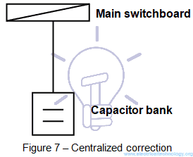
Centralized Power Factor (P.f) correction

De-centralized P.f correction
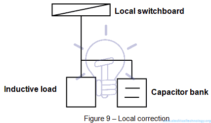
Figure 9 – Local correction
For MV installations capacitor banks may be divided in steps and controlled by a VAr relay or an electronic controller, that monitors and switches steps or the whole capacitor bank based on real time network conditions what is shown in Figure 10, to avoid the supply of reactive power to the network, situation that is also subjected to penalties applied by the electricity distribution companies.
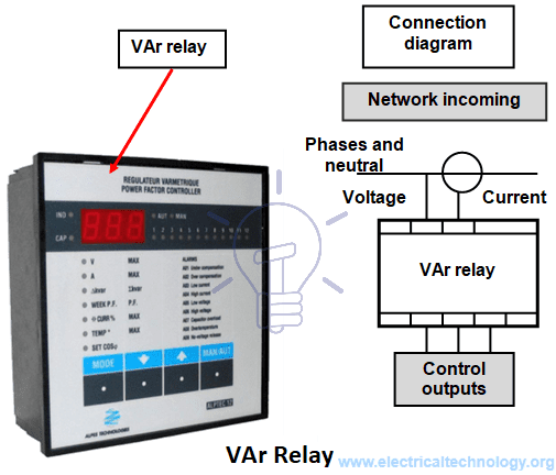
Figure 10 – VAr relay
[1] IEC: International Electrotechnical Commission.
[2] IEEE: Institute of Electrical and Electronic Engineers (USA).
[3] HV: High Voltage (V ≥ 60 kV); MV: Medium Voltage (1 kV < V < 60 kV); LV: Low Voltage (V ≤ 1 kV).
[4] Dielectric absorption is the phenomenon by which a capacitor that has been charged for a long time does not discharges completelywhen submitted to a short discharge.
[5] rms: root mean square.
Read Also


